Internet of things
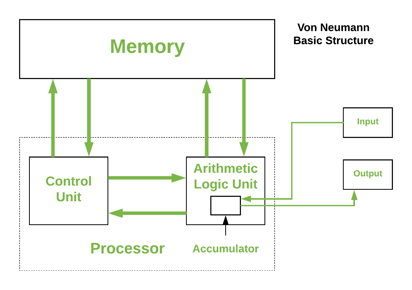
Hardware Layer
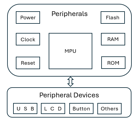
- Microprocessor
- Peripherals
- Peripheral device
Software layer
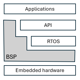
- BSP: Board Support Packet
BSP implemented 2 functionailites, the first is system guide, including MPU initialization, the second is support DDI(Device Driver Interface) to devices and communications between system and peripherals
- RTOS: Real Time Operation System
Scheduler, Storage distribution, Clock management, Interrupts, File/GUI/Net serveices are managed by BASIC KERNEL; Graphics/Automobile/Homekits etc. are managed by EXTENDED KERNEL
- API: Application Programmable Interface
Also referred as middlewares, all software libraries or components are developed at this layer. This layer varies by DDD(Domain Drive Design)
- Softwares
Text editor/Games/Electronic control/Media players etc.
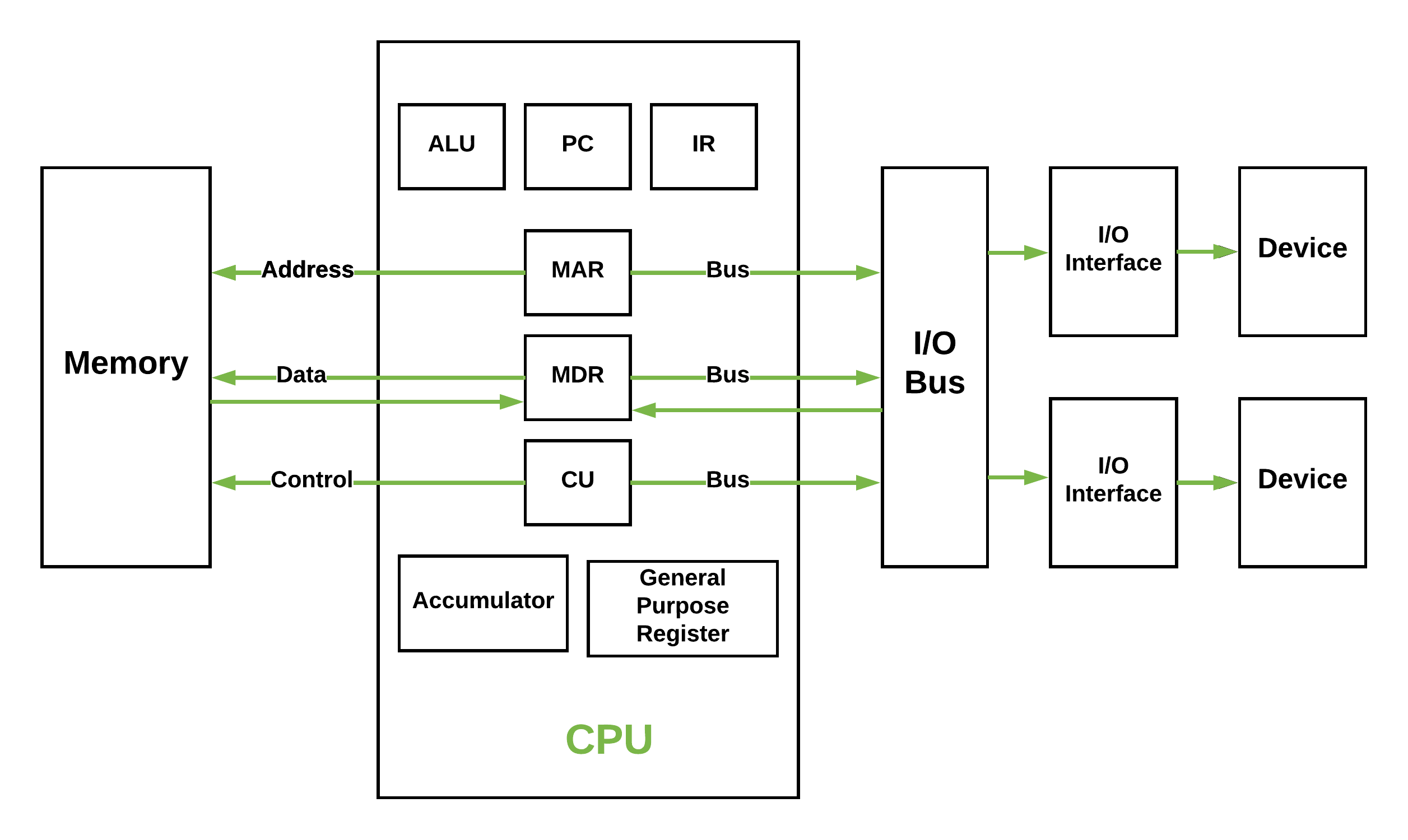
CPU (Centrol Processing Unit)
ALUArithmetic Logic Unit: Performs arithmetic and logical operations (e.g., addition, subtraction, comparisons)PCProgram Counter: Keeps track of the address of the next instruction to be executed.IRorCIRInstruction Register: Holds the current instruction being executed.MARMemory Address Register: Stores the address of the memory location being accessed.MBRMemory Buffer Register: a two-way register that holds data fetched from memory (and ready for the CPU to process) or data waiting to be stored in memoryMDRMemory Data Register: Temporarily holds data being transferred to or from memory.CUControl Unit: Coordinates the activities of the CPU, managing the flow of data and instructions.ACCAccumulator: A register that stores intermediate results of arithmetic and logic operations.General Purpose Registers: Used for temporary storage of data during processing.FPUFloating Point Unit- decoder unit: implements the instruction set either in hardwired form or as a micro program.
ARM Cortex-M7 processor core peripherals
Nested Vectored Interrupt Controller The NVIC is an embedded interrupt controller that supports low latency interrupt processing.
System Control Block The System Control Block (SCB) is the programmers model interface to the processor. It provides system implementation information and system control, including configuration, control, and reporting of system exceptions.
System timer The system timer, SysTick, is a 24-bit count-down timer. Use it as a Real Time Operating System (RTOS) tick timer or as a simple counter.
Integrated instruction and data caches (optional) The instruction and data caches provide fast access to frequently accessed data and instructions, that support increased average performance when using system based memory.
Memory Protection Unit (optional) The Memory Protection Unit (MPU) improves system reliability by defining the memory attributes for different memory regions. Depending on your implementation, it provides up to 8 or 16 different regions, and an optional predefined background region.
Floating-point unit (optional) The FPU provides IEEE754-compliant operations on 32-bit single-precision and implementation-defined 64-bit double-precision floating-point values.
Cortex M7 Processor mode and privilege levels for software execution
The processor modes are:
Thread mode Used to execute application software. The processor enters Thread mode when it comes out of reset.
Handler mode Used to handle exceptions. The processor returns to Thread mode when it has finished all exception processing.
The privilege levels for software execution are:
Unprivileged The software:
- Has limited access to the MSR and MRS instructions, and cannot use the CPS instruction.
- Cannot access the system timer, NVIC, or system control block.
- Might have restricted access to memory or peripherals.
Unprivileged software executes at the unprivileged level.
- Privileged The software can use all the instructions and has access to all resources.
Privileged software executes at the privileged level.
In Thread mode, the CONTROL register controls whether software execution is privileged or unprivileged, see CONTROL register. In Handler mode, software execution is always privileged.
Only privileged software can write to the CONTROL register to change the privilege level for software execution in Thread mode. Unprivileged software can use the SVC instruction to make a supervisor call to transfer control to privileged software.
ARM - Cortex M Core registers
Register data constantly changes, data is loaded in from memroy, results are stored back to memory
Application Binary Interface(ABI) provides architecture details to Compiler/Software Programmer
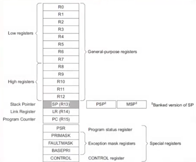
- R0-R12 are 32-bit general-purpose registers for data operations.
- R13 Stack Pointer (SP), In Thread mode, bit[1] of the CONTROL register indicates the stack pointer to use:
0Main Stack Pointer (MSP). This is the reset value.1Process Stack Pointer (PSP). - R14 Link Register, It stores the return information for subroutines, function calls, and exceptions. On reset, the processor sets the LR value to
0xFFFFFFFF. - R15 Program Counter, It contains the current program address. On reset, the processor loads the PC with the value of the reset vector, which is at the initial value of the Vector Table Offset Register (VTOR) plus 0x00000004. Bit[0] of the value is loaded into the EPSR T-bit at reset and must be 1.
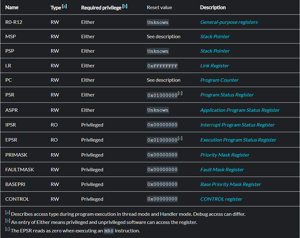
- PSR Program Status Registers
- APSR Application Program Status Register
- IPSR Interrupt Program Status Register
- EPSR Execution Program Status Register

- Exception Mask Registers
- Control Register
- Peripherals, Code, and Data are all represented by 1 address space
Register Definition Files
Platform File that provides interface to peripheral memory by specifying
- Address List for Peripherals
- Access Methods
- Defines for Bit Fields and Bit Masks
Peripheral Access Methods used to read/write data
- Preprocessor Macros
- Direct Dereferencing of Memory
- Structure Overlays
Flash, SRAM, Peripherals, GPIO are platform dependent, details on platform specific registers can be put in C-Programming source files(Register Definition Files)
Compilation tracks and maps memory needs program code and data into segments, which are specified in the Linker file
Use Pointers(address) !!!
Memory Model
data types
- 32-bit words.
- 16-bit halfwords.
- 8-bit bytes.
- 32-bit single-precision floating point numbers if the FPU is implemented.
- 64-bit double-precision floating point numbers if the FPU is implemented.
Manages all data memory accesses as either little-endian or big-endian depending on how your implementation is defined. Instruction memory and Private Peripheral Bus (PPB) accesses are always performed as little-endian
Memory Region, types and attribute
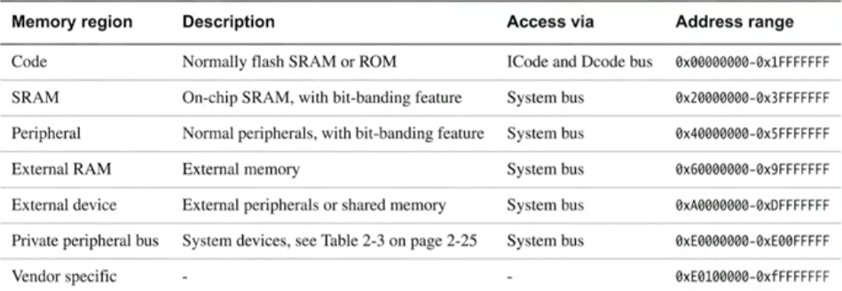
The processor has a fixed default memory map that provides up to 4GB of addressable memory. The memory map is:
Behavior of memory accesses
Memory endianness
Memory-mapped I/O is a technique where peripheral registers are mapped to specific memory addresses in the microcontroller's address space. By reading from and writing to these memory addresses, developers can access and control peripheral functionality directly. memory-mapped peripheral registers in embedded systems are special registers that map physical addresses to control peripheral devices
In embedded systems programming, the memory address of a peripheral register is typically calculated by adding the register's offset (specified in the device datasheet or reference manual) to the base address of the peripheral. This allows direct access to the register's memory location
Memory Map provides a memory address to physical device mapping within an address space for use in programming
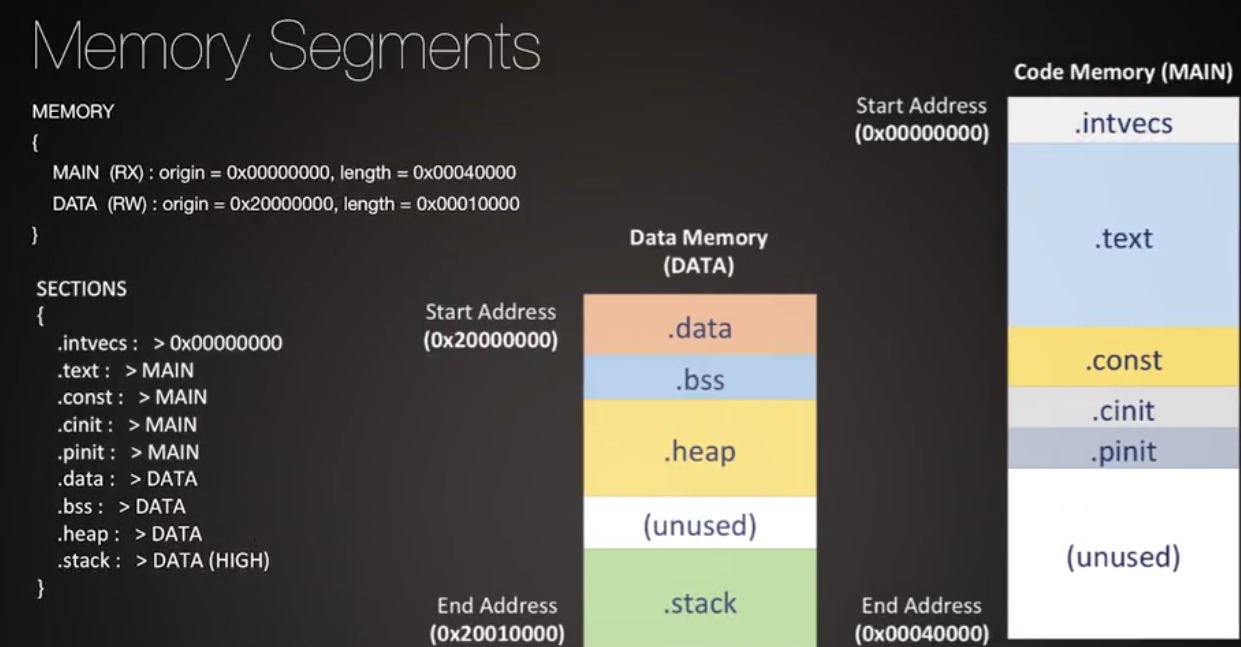
Linker file maps physical memory regions to compiled memory sections, the compiled memory sections of a compiled executable will be relocated by referencing a symbol name. linker file provides physical address to symbol mapping
- Code Memory (Flash)
- Data Memory (SRAM - storing data and variables during program execution)
- System Memory (typically contains the startup code, interrupt vector table, and bootloader)
- Register Memory (internal to chip)
- External Memory (if applicable)
- Peripheral Memory (contains memory-mapped registers for controlling and communicating with various peripherals (e.g., GPIO, UART, SPI))
Memory Hierarchy
*       Registers
**      Cache(L1/L2/L3)
***     RAM(SRAM/DRAM)
****    Flash/EEPROM
*****   HDD(Hard Drives)
******  Tape

Top 4 layer are used in Embedded systems,
layers towards top are expensive, fast(low latency), small capacity,
towards bottom  are cheap, slow(high latency), large capacity
Typically FLASH stores program's code instruction
RAM stores program's data
Memory Segments
Data Segments
- The data segment is a container for the various types of allocated data that get mapped into physical memory
- Four main Sub-segments: Stack, Heap, Data, BSS(Block started by Symbol). each varies with size depending on the program
- Stack: Temporary Data Storage like local variables
- Heap: Dynamic data storage
- Data: Non-zero initialized global and static data
- BSS: Zero initialized and uninitialized global and static data
Data Allocation
- Variable Types:
char,int,float, derived types, enumerated types, _Bool, _Complex(c99) - Type Qualifiers:
const- allocates the data as a constant, will be mapped to Read-Only Memory - Type Modifiers:
unsigned,signed,short,long - Storage Classes:
auto- automatically allocated and deallocated data on the stack, has a lifetime of a function or block,static- data will persist in memory unitl the end of the program, even for local scope variables,extern- declares a global reference defined in another file to be visible by current file,register- allocates data directly in the CPU
int A_BSS:
int B_BSS = 0;
int C_DATA = 1;
const int D_RODATA = 1;

void foo(int E_STACK_REG) {
    int F_STACK_REG;
    int G_STACK_REG = 1;
    static int H_BSS;
    static int I_BSS = 0;
    static int J_DATA = 1;
    char * ptr_STACK_REG;
    ptr_STACK_REG = (char *) malloc(8);
    /* more code */
    free((void *)ptr_STACK_REG);
    return;
}
Memory organization
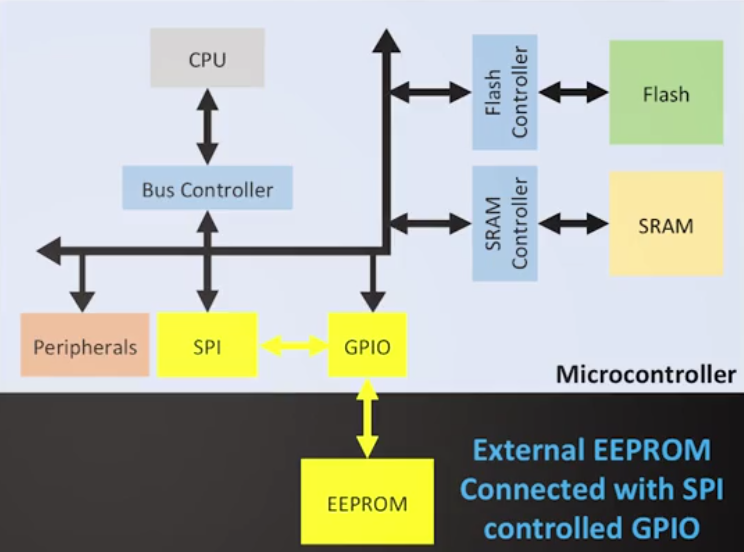
- Flash and SRAM memory requires a controller to manage interface to CPU
- Internal Bus also has a controller
- Additional external memory can be connected through a I/O pins if more memory (EEPROM) is needed
| Volatile Memories | Non-Volatile Memories |
|---|---|
| SRAM | ROM/PROM/EPROM/EEPROM |
| DRAM | FLASH |
| SDRAM | DISK |
| Register(most) | Tape |
- ROM: Read-Only Memory & PROM are programmable once, no ability to write without extra permissions or process
- EPROM: Erasable(UV exposure) and Programmable Multiple times
- EEPROM: Electically Erasable and Programmable Many times
- RAM: Random Access Memory, Allows for access to any part of memory give the address of that location
Interface methods for hardware
- Register Definition Files
- Macro Functions
- Specialized C-Functions
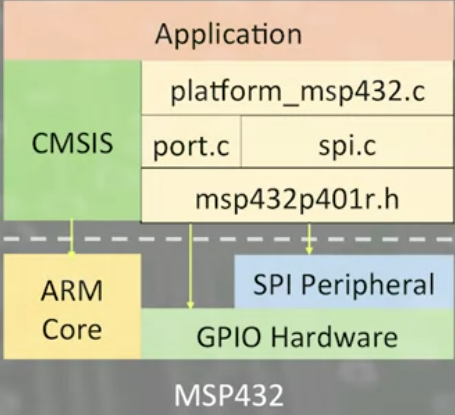
Embedded system architecture
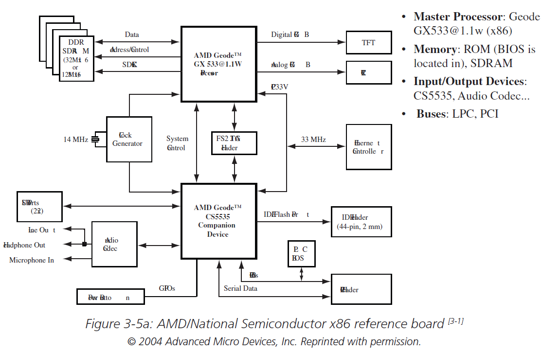
Technical Reference Material
- Datasheet
- Technical Reference manual
- User Guide
- Errata
- Debuggers Users Guide
- Code Composer User Guide
engineering hardware drawings
- Block diagrams
- Schematics (electronic circuti diagrams that provide a more detailed view of all of the devices within a circuit or within a single component)
- Wiring diagrams (bus connections between the major and minor components on a board or within a chip)
- Logic diagrams/prints.
- Timing diagrams.
Sensors Introduction
Platforms
Page Source