ATMEL AT89S51 -> STC89C52RC
AMTEL AT89C52 PORT Pin
| Port Pin | Alternate Functions |
|---|---|
| P1.0 | T2 (external count input to Timer/Counter 2), clock-out |
| P1.1 | T2EX (Timer/Counter 2 capture/reload trigger and direction control) |
| P1.5 | MOSI (used for In-System Programming) |
| P1.6 | MISO (used for In-System Programming) |
| P1.7 | SCK (used for In-System Programming) |
| P3.0 | RXD(serial input port) |
| P3.1 | TXD(serial output port) |
| P3.2 | INT0(external interrupt 0) |
| P3.3 | INT1(external interrupt 1) |
| P3.4 | T0(timer 0 external input) |
| P3.5 | T1(timer 1 external input) |
| P3.6 | WR(external data memory write strobe) |
| P3.7 | RD(external data memory read strobe) |
P0.0~P0.7Port0 :Port0 is an 8-bit bi-directional I/O port with pull-up resistance. Except being as GPIO, Port 0 is also the multiplexed low-order address and data bus during accesses to external program and data memory.P1.0 ~ P1.7Port1 : General-purposed I/O with weak pull-up resistance inside. When 1s are written into Port1, the strong output driving CMOS only turn-on two period and then the weak pull-up resistance keep the port high. P1.0 is also used as one of event sources for timer2, or output carrier of timer 2, alias T2. P1.1 is also used as one of interrupt-controlling sources for time 2, alias T2EX.P2.0 ~ P2.7Port2 : Port2 is an 8-bit bi-directional I/O port with pull-up resistance. Except being as GPIO, Port2 emits the high-order address byte during accessing to external program and data memory.P3.0 ~ P3.7Port3 : General-purposed I/O with weak pull-up resistance inside. When 1s are written into Port1, the strong output driving CMOS only turn-on two period and then the weak pull-up resistance keep the port high. Port3 also serves the functions of various special features. P3.0 and P3.1 act as receiver and transceiver of the data for UART function block, Alias RxD and TxD. P3.2 and P3.3 also act as external interrupt sources, alias /INT0 and /INT1. P3.4 and P3.5 also act as event sources for timer0 and timer1 individually, alias T0 and T1. P3.6 also acts as write signal while access to external memory,alias /WR. P3.7 also acts as read signal while access to external memory, alias /RD.RSTReset input. A high on this pin for two machine cycles while the oscillator is running resets the device. This pin drives High for 96 oscillator periods after the Watchdog times out. The DISRTO bit in SFR AUXR (address 8EH) can be used to disable this feature. In the default state of bit DISRTO, the RESET HIGH out feature is enabled.ALE/PROGAddress Latch Enable (ALE) is an output pulse for latching the low byte of the address during accesses to external memory. This pin is also the program pulse input (PROG) during Flash programming. In normal operation, ALE is emitted at a constant rate of 1/6 the oscillator frequency and may be used for external timing or clocking purposes. Note, however, that one ALE pulse is skipped during each access to external data memory.PSENProgram Store Enable (PSEN) is the read strobe to external program memory. When the AT89S52 is executing code from external program memory, PSEN is activated twice each machine cycle, except that two PSEN activations are skipped during each access to external data memory.EA/VPPExternal Access Enable. EA must be strapped to GND in order to enable the device to fetch code from external program memory locations starting at 0000H up to FFFFH. Note, however, that if lock bit 1 is programmed, EA will be internally latched on reset. EA should be strapped to VCC for internal program executions. This pin also receives the 12-volt programming enable voltage (VPP) during Flash programming.XTAL1Input to the inverting oscillator amplifier and input to the internal clock operating circuit.XTAL2Output from the inverting oscillator amplifier.
I/O Port programming
All port pin on STC89xx series may be independently configured to one of four modes: quasi-bidirectional(standard 8051 port output), push-pull output, input-only or open-drain output
- All the ports upon
RESTare configured as input, ready to be used as input ports - When the first 0 is written to a port, it becomes an output
- To reconfigure it as an input, a 1 must be sent to the port
- P0 is an open drain, unlike P1, P2, and P3
- Port 3 has the additional function of providing some extremely important signals
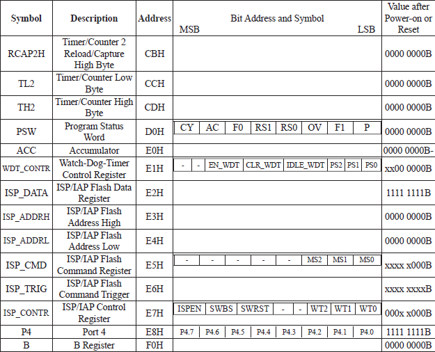
Special Function Registers
A map of the on-chip memory area called the Special Function Register (SFR)
AccumulatorACC is the Accumulator register. The mnemonics for accumulator-specific instructions, however, refer to the accumulator simply as AB RegisterThe B register is used during multiply and divide operations. For other instructions it can be treated as another scratch pad register.PSWThe program status word contains several status bits that reflect the current state of the CPU. The PSW, shown below, resides in the SFR space. It contains the Carry bit, the Auxiliary Carry(for BCD operation), the two register bank select bits, the Overflow flag, a Parity bit and two user-definable status flags. The Carry bit, other than serving the function of a Carry bit in arithmetic operations, also serves as the “Accumulator” for a number of Boolean operations. The bits RS0 and RS1 are used to select one of the four register banks shown in the previous page. A number of instructions refer to these RAM locations as R0 through R7. The Parity bit reflects the number of 1s in the Accumulator. P=1 if the Accumulator contains an odd number of 1s and otherwise P=0.
Stack PointerThe Stack Pointer register is 8 bits wide. It is incremented before data is stored during PUSH and CALL executions. While the stack may reside anywhere in on-chip RAM, the Stack Pointer is initialized to 07H after a reset. This causes the stack to begin at location 08HData PointerThe Data Pointer (DPTR) consists of a high byte (DPH) and a low byte (DPL). Its intended function is to hold a 16-bit address. It may be manipulated as a 16-bit register or as two independent 8-bit registers. For fast data movement, STC89xx series support two data pointers. They share the same SFR address and are switched by the register bit – DPS/AUXR1.0.
Ports 0 to 3P0, P1, P2 and P3 are the SFR latches of Ports 0, 1, 2 and 3, respectively.Serial Data BufferThe Serial Data Buffer is actually two separate registers, a transmit buffer and a receive buffer register. When data is moved to SBUF, it goes to the transmit buffer where it is held for serial transmission. (Moving a byte to SBUF is what initiates the transmission.) When data is moved from SBUF, it comes from the receive buffer.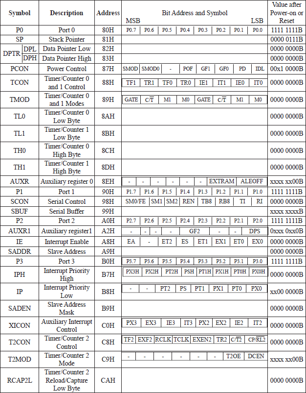
Addressing Modes
The CPU can access data in various ways, which are called addressing modes, Addressing modes are an integral part of each computer’s instruction set. They allow specifying the source or destingation of data in different ways, depending on the programming situation. There eight modes available:
- Register
- Direct
- Indirect
- Immediate
- Relative
- Absolute
- Long
- Indexed
Program Memory
- has total of 128k bytes of memory space
- 64k bytes of code and 64k bytes of data, the code space are accessed using instruction
MOVC A, @A+DPTR, while the data memeory space is accessed using the DPTR register and an instruction calledMOVX, where X stands for external - the data space cannot be shared between code and data
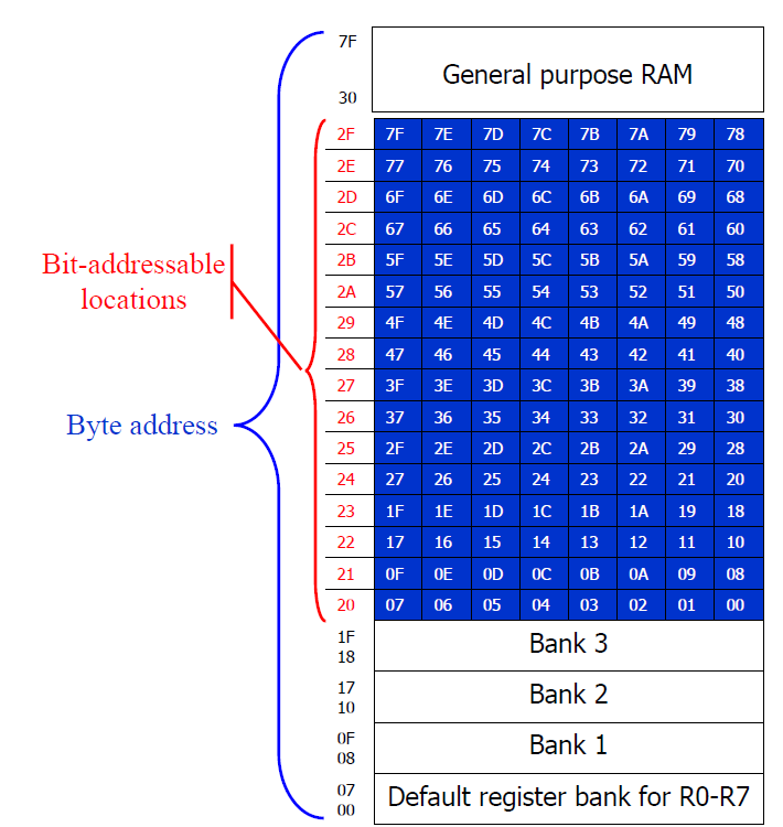
- in many applications we use RAM locations
30H-7FHas scratch pad - we use
R0~R7of bank 0, leaves addresses08H-1FHfor stack usuage - if we need more registers, we simply use RAM locations
30H-7FH - it is registers, RAM, and I/O ports that need to be bit-addressable
- ROM, holding program code for execution, is not bit-addressable
- 8K
0000H ~ 1FFFH
Data types
| Data Type | Size in Bits | Data Range/Usuage |
|---|---|---|
unsigned char |
8-bit | 0~255 |
(signed) char |
8-bit | -128~+127 |
unsigned int |
16-bit | 0 ~ 65535 |
(signed) int |
16-bit | -32768~+32767 |
| sbit | 1-bit | SFR bit-addressable only |
| bit | 1-bit | RAM bit-addressalbe only |
| sfr | 8-bit | RAM addresses 80H-FFH only |
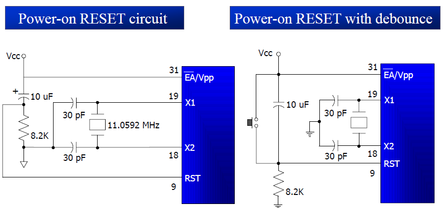
Power-on Reset
Upon applying a high pulse to REST(Pin 9), the microcontroller will reset and terminate all activites, this is often referred to as a power-on reset
- In order for the RESET input to be effective, it must have a minimum duration of 2 machine cycles.
- All the ports upon RESET are configured as output, ready to be used as input ports
- Port 0 is also designated as AD0-AD7, allowing it to be used for both address and data
- when connecting an 8051/31 to an external memory, port 0 provides both address and data
- ALE indicates if P0 has address or data, when ALE=0, it provides data D0-D7; when ALE=1, it has address A0-A7
| Register | Reset Value |
|---|---|
| PC | 0000 |
| DPTR | 0000 |
| ACC | 00 |
| PSW | 00 |
| SP | 07 |
| B | 00 |
| P0-P3 | FF |
TMOD
TMOD is a 8-bit register, the lower 4 bits are for Timer 0, the upper 4 bits are for Timer 1, In each case, the lower 2 bits are used to set the timer mode, the upper 2 bits to specify the operation
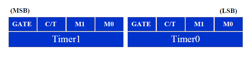
| M1 | M0 | Mode | Operating Mode |
|---|---|---|---|
| 0 | 0 | 0 | 13-bit timer mode, 8-bit timer/counter THx with TLx as 5-bit prescaler |
| 0 | 1 | 1 | 16-bit timer mode, 16-bit timer/counter THx and TLx are cascaded; there is no prescaler |
| 1 | 0 | 2 | 8-bit auto reload, 8-bit auto reload timer/counter; THx holds a value which is to be reloaded TLx each time it overflows |
| 1 | 1 | 3 | Split timer mode |
- In using software to start and stop the timer where GATE=0, the start and stop of the timer are controlled by way of software by the TR(timer start) bits TR0 and TR1
- The hardware way of starting and stopping the timer by an external source is achieved by making GATE=1 in the TMOD register
- The C/T bit in the TMOD registers decides the source of the clock for the timer, when C/T=1, the timer is used as a counter and gets its pulses from outside the 8051, The counter counts up as pulses are fed from pins 15 and 15, these pins are called T0(timer 0 input) and T1(timer 1 input)
mode1 characteristics
- It is a 16-bit timer; therefor it allows value of 0000H to FFFFH to be loaded into the the timer’s register TL and TH
- After TH and TL are loaded with a 16-bit initial value, the timer must be started. This is done by the instruction
SETB TR0for timer 0 andSETB TR1for timer 1 - After the timer is started, it starts to count up, unitl it reaches its limit of FFFFH, when it rolls over from FFFFH to 0000H, it sets high a flog bit called TF(timer flag, TF0 for timer 0, TF1 for timer 1), when this timer flag is raised, one option would be to stop the timer with the instructions
CLR TR0orCLR TR1, for timer 0 and timer 1, respectively - After the timer reaches its limit and rolls over, in order to repeat the process: TH and TL must reloaded with the original value, and TF must be reloaded to 0
// Task: use Timer 0, mode 1(16-bit) to create 50ms delay
#include <reg51.h>

// in 8051, the machine cycle frequency is always of 1/12 of the XTAL frequency, therefore
// 11.0529MHz / 12 = 921.6kHz;
// T = 1/921.6kHz = 1.085μs

void T0M1_Delay(void) {
  TMOD=0x01; // set TMOD as mode 1(16-bit) as timer
  TL0=0xFD; // set initial value of low 8-bit
  TH0=0x4B; // set initial value of high 8-bit, together is 4BFDH
  // FFFFH - 4BFDH = B402H = 46082 + 1(wait until flag is set) = 46083
  // 46083 x 1.085μs = 50ms
  TR0=1; // start the timer
  while (TF0==0); // wait unitl TF is set by HW
  TR0=0; // reset start
  TF0=0; // reset flag
}
mode2 characteristics
- It is an 8-bit timer; therefor, it allows only values of 00H to FFH to be loaded into the timer’s register TH
- After TH is loaded with the 8-bit value, the 8051 gives a copy of it to TL, then the timer must be started, this is done by the instruction
SETB TR0for timer 0 andSETB TR1for timer 1 - After the timer is started, it starts to count up by incrementing the TL register, it counts up until it reaches its limit of FFH, when it rolls over from FFH to 00H, it sets high the TF(timer flag)
- When the TL register rolls from FFH to 0 and TF is set to 1, TL is reloaded automatically with the original value kept by the TH register. To repeat the process, we must simply clear TF and let it go without any need by the programmer to reload the original value. This makes mode 2 an auto-reload, in contrast with mode 1 in which the programmer has to reload TH and TL
// Task: Use Timer 0, mode 2 (8-bit auto-reload) create 250ms delay continuously toggle pin P1.5
#include <reg51.h>

void T0M2_Delay(void);
sbit mybit = P1^5;
void main(void) {
  unsigned char x,y;
  while (1) {
    mybit = ~mybit;
    for (x=0;x<250;x++) // 25μs x 250 x 40 = 250ms
      for (y=0;y<36;y++) // Due to overhead of the for loop in C, we put 36 instead of 40
        T0M2_Delay();
  }
}

void T0M2_Delay(void) {
  TMOD = 0x02; // use Timer 0, mode 2
  TH0 = -23; // set initital value of TH0
  // 23 x 1.085μs = 25μs
  TR0 = 1; // start timer
  while (TF0 == 0); // wait unitl TF0 is set by HW
  TR0 = 0; // reset start
  TF0 = 0; // reset flag
}
// Task: create a frequency of 2500Hz on pin P2.7, use Timer 1, mode 2 to create delay
#include <reg51.h>
// 1/2500Hz = 400μs
// 400μs /2 = 200μs
// 200μs / 1.085μs = 184

void T1M2_Delay(void);
sbit mybit = P2^7;
void main(void) {
  unsigned char x;
  while (1) {
    mybit = ~mybit;
    T1M2_Delay();
  }
}
void T1M2_Delay(void) {
  TMOD = 0x20; // use Timer 1, mode 2;
  TH1 = -184; // set initial value: 0x48
  TR1 = 1; // start timer
  while (TF1 == 0); // wait until time flag is set by HW
  TR1 = 0; // reset start
  TF1 = 0; // reset flag
}
SCON
SCON is an 8-bit register used to program the start bit, stop bit, and data bits of data framing, among other things
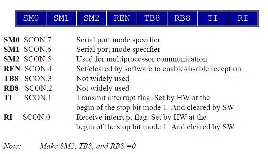
| SM0 | SM1 | Mode |
|---|---|---|
| 0 | 0 | Serial mode 0 |
| 0 | 1 | Serial mode 1, 8-bit data, 1 stop bit, 1 start bit |
| 1 | 0 | Serial mode 2 |
| 1 | 1 | Serial mode 3 |
Transmitting, TI(transfer interrupt) is raised when the last bit of the framed data, the stop bit, is transferred, indicating that the SBUF register is ready to transfer the next byte
- TMOD register is loaded with the value
20H, indicating the use of timer 1 in mode 2(8-bit auto-reload) to set baud rate - The TH1 is loaded with one of the values to set baud rate for serial data transfer
- The SCON register is loaded with the value
50H, indicating serial mode 1, where an 8-bit data is framed with start and stop bits - TR1 is set to 1 to start timer 1
- TI is cleared by
CLR TIinstruction - The character byte to be transfered serially is written into SBUF register
- The TI flag bit is monitored with the used of instruction
JNB TI, xxto see if the character has been transferred completely - To tranfer the next byte, go to step 5.
        MOV TMOD,#20H     ;timer 1,mode 2(auto reload)
        MOV TH1,#-6       ;4800 baud rate
        MOV SCON,#50H     ;8-bit, 1 stop, REN enabled
        SETB TR1          ;start timer 1
AGAIN:  MOV SBUF,#”A”     ;letter “A” to transfer
HERE:   JNB TI,HERE       ;wait for the last bit
        CLR TI            ;clear TI for next char
        SJMP AGAIN        ;keep sending A
Receiving, RI(received interrupt) is raised when the entire frame of data, including the stop bit, is received
- TMOD register is loaded with the value
20H, indicating the use of timer 1 in mode 2 (8-bit auto-reload) to set baud rate - TH1 is loaded to set baud rate
- The SCON register is loaded with the value
50Hindicating serial mode 1, where an 8-bit data is framed with start and stop bits - TR1 is set to 1 to start timer 1
- RI is cleared by
CLR RIinstruction - The RI flag bit is monitored with the use of instruction
JNB RI, xxto see if an entire character has been received yet - When RI is raised, SBUF has the byte, its contents are moved into a safe place
- To receive the next character, go to step 5
        MOV TMOD,#20H         ;timer 1,mode 2(auto reload)
        MOV TH1,#-6           ;4800 baud rate
        MOV SCON,#50H         ;8-bit, 1 stop, REN enabled
        SETB TR1              ;start timer 1
HERE:   JNB RI,HERE           ;wait for char to come in
        MOV A,SBUF            ;saving incoming byte in A
        MOV P1,A              ;send to port 1
        CLR RI                ;get ready to receive next
                              ;byte
        SJMP HERE             ;keep getting data
ATMEL 80C51 CPU Timing
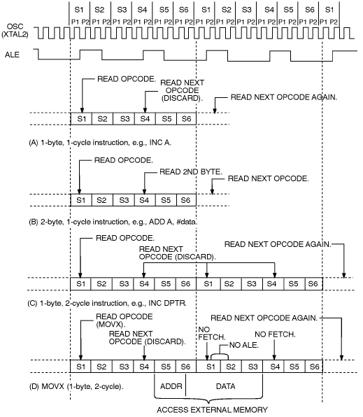
A machine cycle consists of 6 states (12 oscillator periods). Each state is divided into a
Phase 1 half, during which the Phase 1 clock is active, and a Phase 2 half, during which
the Phase 2 clock is active. Thus, a machine cycle consists of 12 oscillator periods,
numbered S1P1 (State 1, Phase 1), through S6P2 (State 6, Phase 2). Each phase lasts
for one oscillator period. Each state lasts for two oscillator periods. Typically, arithmetic
and logical operations take place during Phase 1 and internal register-to-register transfers
take place during Phase 2.
The diagrams above show the fetch/execute timing referenced to the internal
states and phases. Since these internal clock signals are not user accessible, the
XTAL2 oscillator signal and the ALE (Address Latch Enable) signal are shown for external
reference. ALE is normally activated twice during each machine cycle: once during
S1P2 and S2P1, and again during S4P2 and S5P1.
Execution of one-cycle instruction begins at S1P2, when the opcode is latched into the
Instruction Register. If it is a two-byte instruction, the second byte is read during S4 of
the same machine cycle. If it is one-byte instruction, there is still a fetch at S4, but the
byte read (which would be the next opcode), is ignored, and the Program Counter is not
incremented. In any case, execution is complete at the end of S6P2. Figure A and
Figure B show the timing for a 1-byte, 1-cycle instruction and for a 2-byte, 1-cycle
instruction.
Most 80C51 instructions execute in one cycle. MUL (multiply) and DIV (divide) are the
only instructions that take more than two cycles to complete. They take four cycles.
Separately, two codes bytes are fetched from Program Memory during every machine
cycle. The only exception to this is when a MOVX instruction is executed. MOVX is a 1-
byte 2-cycle instruction that accesses external Data Memory. During a MOVX, two
fetches are skipped while the external Data Memory is being addressed and strobed.
Figure C and Figure D show the timing for a normal 1-byte, 2-cycle instruction
and for a MOVX instruction.
Development
- Code Editor(windows) - Keil uVision5
- Compiler - Uploader STC-ISP
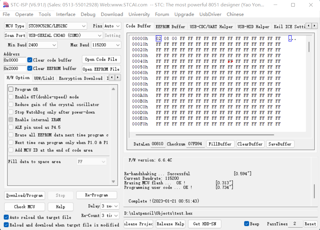
Checking target MCU ...
  MCU type: STC89C52RC/LE52RC
  F/W version: 6.6.4C

Current H/W Option:
  . Current clock frequency: 11.030MHz
  . System use 12T mode
  . Oscillator gain is HIGH
  . Any reset source can stop WatchDog if WatchDog timer is running
  . Internal XRAM is ENABLE
  . ALE pin behaves as ALE function pin
  . Do not detect the level of P1.0 and P1.1 next download
  . Do not erase user EEPROM area at next download

  MCU type: STC89C52RC/LE52RC
  F/W version: 6.6.4C


Re-handshaking ... Successful			[0.594"]
Current Baudrate: 115200
Erasing MCU flash ...  OK !		[0.313"]
Programming user code ... OK !		[0.734"]


  Complete !(2023-01-21 10:51:43)